Manufacturing process of CNT-TFT 2025 edition


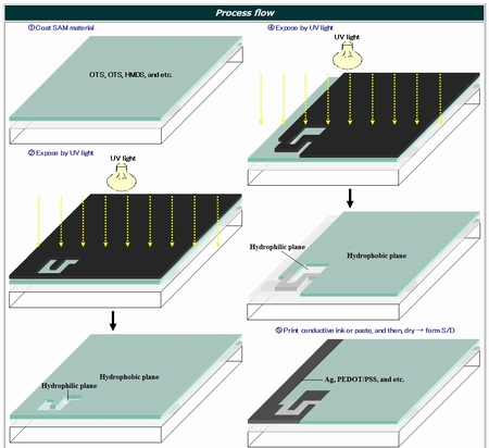
■Explain CNT-TFT manufacturing process by illustration
■Full-cover from basic process to next generation process
■Cover structure, substrate, material, and manufacturing process
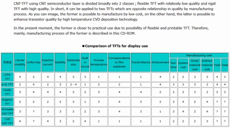
■Clearly difference of printable TFT and high quality TFT, which are main kinds of CNT-TFT
■In the CNT semiconductor layer process, the detail processes from pre-treatment to CVD/wet coating process are explained

■Easy to look at the file using any PC because of the format of browser, for example IE (Internet Explorer)
■Possible to access at will from Index Page to detail page

■Describe these illustrations at 3D image
■Number of total file are 35 (about 80 page in A4 form equivalent)
■Illustrations of device structure and process flow are approximately 190.

CONTENT


Structure of CNT-TFT
  Bottom contact type
  Top contact type
  Flexible CNT-TFT
  Transparent CNT-TFT

Manufacturing process of bottom contact CNT-TFT (General theory)
Manufacturing process of top contact CNT-TFT (General theory)

Forming process of gate electrode
  In the case of using vacuum deposited film
  In the case of using wet type material

Forming process of gate insulator film
  In the case of use of organic material, wettable inorganic material
  In the case of use of inorganic material
  In the case of use of TaOx
  In the case of use of AlOx+SAM

Forming process of S/D electrode
  In the case of inorganic material (Dry-coating method)
  In the case of wettable material
  In the case of CNT

Forming process of transparent pixel electrode
  In the case of transparent oxide material
  In the case of metal material
  In the case of wettable material (Conductive polymer, CNT, and Nano size Ag)

Forming process of CNT semiconductor layer
  In the case of the CVD method
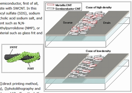
  In the case of wet-coating method (SAM treatment, Separation and elimination of metallic SWCNT, Wet-coating method)

Co-forming process of S/D and CNT semiconductor layer by use of SAM

Forming process of passivation layer

A word of caution in manufacturing of CNT-TFT with flexible substrate
  Case of using flexible substrate with film shape
  CNT-TFT and device are manufactured on original substrate, and then transferred to plastic film
  Resin is coated on support substrate and cured, and then, CNT-TFT and device are manufactured on resin film, finally, support substrate is released (the resin film is used as substrate)


Full-original Data

Media:CD-ROM or USB memory
Price:19,000 yen
Release date:January 4th 2025

While you order this CD-ROM, please input below points and send to info@e-express.co.jp.

CD-ROM:CNT-TFT manufacturing process
Campany's Name:
Section:
Name:
Address:
TEL:
FAX:
e-mail address:
Media:CD-ROM or USB memory (Please erase CD-ROM or USB memory.)

Remark

If you are domestic customer, we will send the product and invoice. Please pay to ours account by bank remittance until specified date.

If you are overseas customer, we will send E-mail to you. Please pay to ours account by bank remittance. If we confirm bank transfer, we send the product immediately.


E Express Inc.
TEL:+81-90-4203-4633(Kameya(President))
E-Mail:info@e-express.co.jp

CD-ROM lists of English virsion

Manufacturing process of LTPS-TFT-LCD Manufacturing process of oxide-TFT-LCD
Manufacturing process of a-Si TFT-LCD Manufacturing process of oxide-TFT
Manufacturing process of OLED Manufacturing process of OLED lighting device
Manufacturing process of organic film solar cell Manufacturing process of E-paper display
Manufacturing process of FEL Manufacturing process of organic-TFT
Manufacturing process of CNT-TFT Manufacturing process of Perovskite solar cell

Go to the top page