üĪStructure of LTPS-TFT-LCD
ć@Single drain structure (SD)
ćADual Gate structure
ćBLDD (Lightly Doped Drain) structure
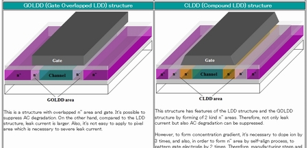
ćCGOLDD (Gate Overlapped LDD) structure
ćDCLDD (Compound LDD) structure
üĪCrystallization process
üĪTFT array process
ć@Single drain structure (SD)
ćALDD (Lightly Doped Drain) structure
ćBGOLDD (Gate Overlapped LDD) structure
ü@
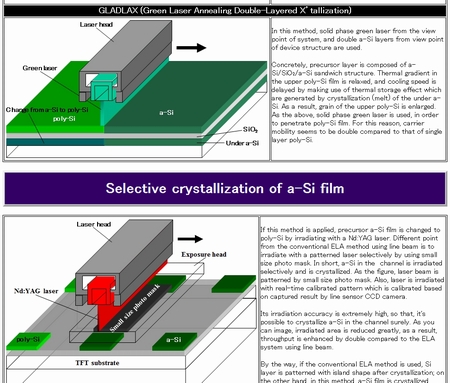
Forming process of poly-Si
ü@
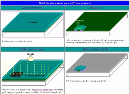
Forming process of TFT area (PEP1)
ü@
Batch forming process of S/D in TFT area and N-channel (PEP1)
ü@
High concentration P doping process (PEP2)
ü@
Forming process of gate electrode and capacitor electrode (PEP3)
ü@
P-TFT High concentration N doping process (PEP4)
ü@
Forming process of contact hole (PEP5)
ü@
Forming process of data line (PEP6)
ü@
Hydrotreatment, form passivation and planarization layer (PEP7)
ü@
Manufacturing process of pixel electrode (PEP8)
ü@
P-TFT ion doping process
ü@
N-TFT ion doping process
üĪCF (Color filter) forming process
ü@
Manufacturing process of CF for IPS mode/FFS mode TFT-LCD
ü@
Manufacturing process of CF for VA mode TFT-LCD
ü@
Manufacturing process of CF for TN/OCB mode TFT-LCD
ü@ü@
Black matrix forming process
ü@ü@
Manufacturing process of R, G, B color layer
ü@ü@
Manufacturing process of overcoat layer
ü@ü@
Deposition process of opposite electrode
ü@ü@
Manufacturing process of post-spacer
ü@ü@
Manufacturing process of rib (bump)
ü@ü@
Photo-alignment process (for MVA mode TFT-LCD)
üĪLC cell process
ü@
Polyimid coating process
ü@
Alignment process
ü@
Seal layer forming process
ü@
Dispersion process of spacer-ball
ü@
Making panel thinner process
ü@
Scribe and break process
ü@
Filling process of LC material
ü@
ODF (One drop fill) process
üĪModule assemble process
ü@
Connect panel and driver-IC
üĪLiquid crystal material and display mechanism
üĪStructure of backlight module
üĪ3D technology
Method to use a specific glasses
ü@
LC shutter glasses method (Time sequential method)
ü@
Polarized glasses ü{ patterned phase difference film (Space division method)
Specific glasses-free method
ü@
Parallax barrier method
ü@
Parallax barrier using dual emission OLED
ü@
Time sequential driving ü{ parallax LC barrier method
ü@
Lenticular lens method
ü@
Time sequential twin-lens 3D-OCB method
ü@
Lenticular ü{ time sequential scanning backlight method
Detail of material and system is explained |


