Manufacturing process of FEL 2025 edition


¡Explain FEL (Field Emission Lamp) manufacturing process by illustration
¡Cover structure, classification, and manufacturing process
¡Full-cover from basic process to next generation process
¡Describe various emitters such as CNT, CNW, BSD, CNC, and etc.

¡Easy to look at the file using any PC because of the format of browser, for example IE (Internet Explorer)
¡Possible to access at will from Index Page to detail page
¡Describe these illustrations at 3D image
¡Number of total file are 27 (about 80 page in A4 form equivalent)
¡Illustrations of device structure and process flow are approximately 120.

MAIN CONTENT


¡Significance of existence of FEL

¡Classification of FEL

¡Structure of FEL and design concept

¡Manufacturing process of FEL (general theory)
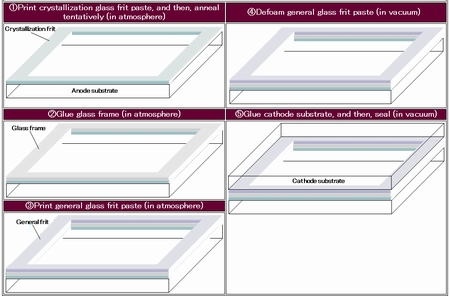
@ Manufacturing process of diode structure FEL
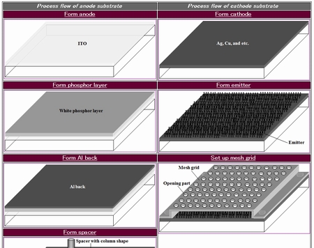
@ Manufacturing process of triode structure FEL

¡Manufacturing process of FEL (particular theory)
@ Forming process of transparent anode
@ Forming process of phosphor layer
@ Forming process of Al back
@ Forming process of spacer
@ Forming process of seal layer
@ Forming process of cathode
@ Kind of emitter and manufacturing process
@ Single wall carbon Nano tube
@ Multi wall carbon Nano tube (MWCNT)
@ Carbon Nano tube with metal
@ Carbon Nano coil (CNC)
@ Carbon Nano twist
@ Cup-stacking type CNT
@ Carbon Nano wall (CNW)
@ Nano diamond
@ Whisker
@ BSD (Ballistic electron Surface emitting Display)
@ BLD (Ballistic Lighting Display)
@ Electride ceramics emitter
@ FEED (Ferroelectric Electron Emitter Device)
@ Mounting process of mesh grid
@ Baking process and outgassing process
@ Assemble, seal, exhaust, and activate process


£Process flow of triode type FEL


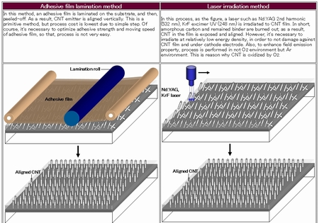
£Activation process of CNT emitter


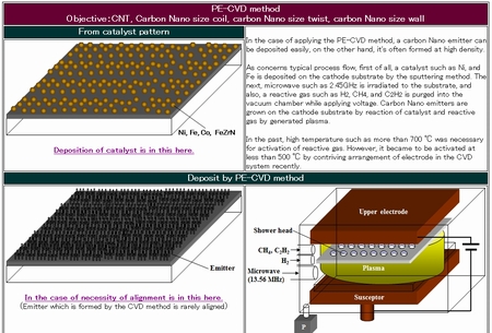
£Deposition process of CNT emitter

Full-original Data

MediaFCD-ROM or USB memory
PriceF19,000 yen
Release dateFJanuary 4th 2025

While you order this CD-ROM, please input below points and send to info@e-express.co.jp.

CD-ROMF FEL manufacturing process
Campany's NameF
SectionF
NameF
AddressF
TELF
FAXF
e-mail addressF
MediaFCD-ROM or USB memory (Please erase CD-ROM or USB memory.)

Remark

If you are domestic customer, we will send the product and invoice. Please pay to ours account by bank remittance until specified date.

If you are overseas customer, we will send E-mail to you. Please pay to ours account by bank remittance. If we confirm bank transfer, we send the product immediately.

E Express Inc.
TELF+81-90-4203-4633(Kameya(President))
E-MailFinfo@e-express.co.jp

CD-ROM lists of English virsion

¡Manufacturing process of LTPS-TFT-LCD ¡Manufacturing process of oxide-TFT-LCD
¡Manufacturing process of a-Si TFT-LCD ¡Manufacturing process of oxide-TFT
¡Manufacturing process of OLED ¡Manufacturing process of OLED lighting device
¡Manufacturing process of organic film solar cell ¡Manufacturing process of E-paper display
¡Manufacturing process of FEL ¡Manufacturing process of organic-TFT
¡Manufacturing process of CNT-TFT ¡Manufacturing process of Perovskite solar cell

Go to the top page

@